plasma technology GmbH logo
Contact

Avoid the regulatory and environmental risks associated with fluorinated greenhouse gases.

For companies in the semiconductor and PCB industries, transitioning to this zero-emission process is not just an environmental choice but a strategic necessity.

As international regulations (like the Kigali Amendment) begin to restrict the use of F-gases, traditional etching will become more expensive and legally fraught.

This closed-loop system offers a way to maintain high-quality technical results while completely removing the regulatory and environmental risks associated with fluorinated greenhouse gases and reducing operating costs.

Note PCB and wafer Etching / Ashing:-
Maintain process efficiency and reduce operating costs.

For more technical specifics or to discuss implementation, please contact plasma technology GmbH directly.

Plasma etching zero perfluorinated hydrocarbon emissions system schematic

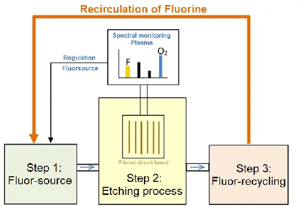
Plasma etching - zero perfluorinated hydrocarbon emissions system overview

The technology, developed through the "PlasmaKlient" research project (a collaboration between plasma technology GmbH and Furtwangen University), introduces a multi-stage, hermetically sealed, recirculating low-pressure plasma process.

Its primary goal is to eliminate the emission of perfluorinated hydrocarbons (HFCs, F-gases, and PFCs) during the etching of printed circuit boards (PCBs) and semiconductor wafers.

These gases are notorious for having a global warming potential (GWP) up to 12,200 times higher than CO2.

Why Choose Closed-Loop Plasma Etching from plasma technology GmbH ?

Environmental Impact

Traditional Etching

High emissions of GWP gases (CF4, C2F6, etc.) thousands of times more potent than CO2.

New Closed-Loop Etching

Zero perfluorinated hydrocarbon emissions.

Business Reasoning

Aligns with CSR and significantly reduces corporate carbon footprint.

Regulatory Compliance

Traditional Etching

High risk. Kigali agreement mandates 85% reduction in HFCs by 2036.

New Closed-Loop Etching

Future-proof. Exceeds international climate regulations.

Business Reasoning

Avoids future fines, carbon taxes, or forced production halts.

Process Stability

Traditional Etching

Reliable, but dependent on external gas supply chains.

New Closed-Loop Etching

High stability. Controlled multi-stage recirculating process.

Business Reasoning

Maintains precision for complex PCB and semiconductor structures.

Alternative Gases

Traditional Etching

HFC-free substitutes often result in poor etch rates and unstable results.

New Closed-Loop Etching

Uses reactive fluorine generated in-situ from a solid target. Significantly reducing operating costs.

Business Reasoning

Prevents quality degradation associated with standard "green" substitutes.

Long-term Viability

Traditional Etching

Low. Faces danger of emission limits becoming a production barrier.

New Closed-Loop Etching

High. Ensures viability of dry etching in a regulated market.

Business Reasoning

Secures the supply chain and production capability against gas phase-outs.

Future proof your PCB and Wafer production and save costs

Take the first step now:

Market focus: Semiconductor and circuit board industries.

Dry plasma etching used increasingly in these industries resulting in considerable amounts of fluorinated greenhouse gases being released.

Who should be considering this?

Multi layer circuit board manufacturers

Plasma etching also known as plasma ashing is used for etching back circuit layers in multilayer PCB assemblies, surface activation and structuring, or cleaning holes for through-hole plating (Desmearing).

Semiconductor industries

For substrate structuring and also for cleaning CVD coating equipment.

Background

There is a great danger that the necessary HFC emission reductions for the printed circuit board and semiconductor industry will soon become a very real problem - not only in Europe, but worldwide.

Reducing these risks has become a major consideration for companies in the semiconductor and PCB industries