Plasma etching for Desmearing PCBs
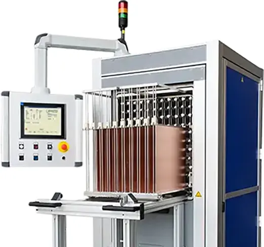
Plasma Technology GmbH manufacture a range Plasma etchers that provides a clean, precise, and eco-friendly method for ensuring high-quality vias and reliable multilayer interconnections.
Our experienced engineers provide support with process optimization helping with the selection of process gases and process parameters to ensure process uniformity.
The industrial computers ensure repeatability, monitoring and documentation of the process.
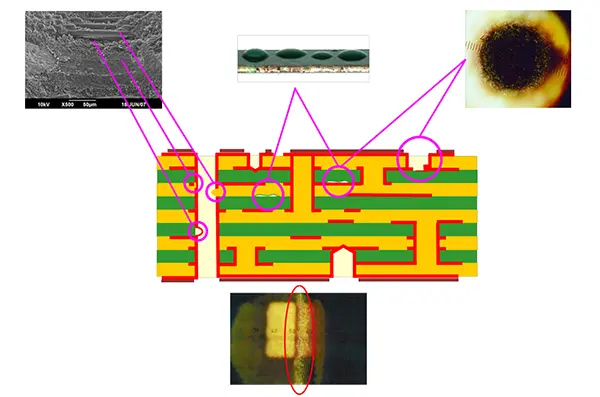
Desmearing is a key step for ensuring reliable electrical connections between PCB layers.
These residues can:
- impair electrical connections between layers,
- reduce the adhesion of the plated copper inside the via,
- lead to open or high-resistance connections.
There are three methods which are commonly used.
- Plasma
- Chemical
- Mechanical.
Plasma etching brings a number of advantages as a desmearing process:-
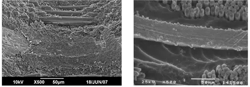
Superior Resin Removal
- Effectively removes resin smear without damaging copper inner layers.
- Ensures clean via walls, improving electrical conductivity.
Non-Destructive Process
- Unlike chemical methods, plasma does not etch or weaken the copper.
- Ideal for high-density PCBs with fine pitch vias.
Uniform and Controlled Cleaning
- Provides consistent Desmearing across all vias, regardless of board complexity.
- No risk of over-etching or uneven material removal.
Compatible with Various PCB Materials
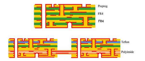
- Works well with FR4, polyimide, PTFE, and other advanced substrates.
- Ideal for RF, microwave, and high-frequency PCBs.
Environmentally Friendly
- No hazardous chemicals like potassium permanganate are used.
- Reduces waste disposal costs and improves workplace safety.
Ideal for Small and Blind Vias
- Plasma can reach microvias, blind vias, and buried vias where wet chemistry struggles.
- Essential for HDI (High-Density Interconnect) PCBs.
Enhanced Copper Adhesion
- Improves surface activation, leading to better adhesion of electroless copper plating.
- Enhances via reliability and long-term performance.


