Innovation: Zero-Emission Etching
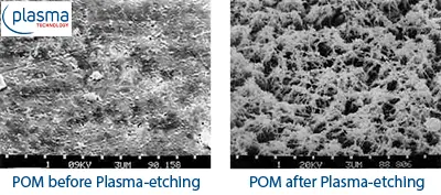
PCB Fabrication & Desmearing
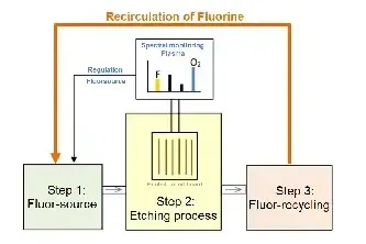
Traditional etching uses perfluorinated hydrocarbon gases that are costly and environmentally taxing. Our proprietary technology changes the game by significantly improving the environmental friendliness of the plasma etching processes and thus ensure the long-term viability of plasma etching.
Fluorine Recirculation
Our system generates its own gases and recovers them for reuse. This eliminates environmental emissions and slashes operational costs.
View Recovery Technology